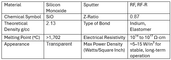
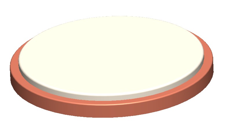
Ideal Vacuum Circular Magnetron Sputtering Targets, SILICON MONOXIDE- SiO Sputtering Target, 3'' Diameter x 0.25" Thick, 99.99 Percent Purity, Metallic Bonded to a 0.125" OFHC Copper Backing Plate.
Ideal Vacuum Products, LLC.
This product is a circular magnetron SILICON MONOXIDE- SiO sputtering target, with a 3'' diameter x 0.25" thickness. It is 99.99% pure, and is metallically bonded to a 0.125" OFHC (Oxygen-Free High Conductivity) copper backing plate.
We use a very competitive pricing strategy to ensure you receive the highest quality products at the best possible value, giving you both affordability and excellence in every purchase. We offer huge discounts to every customer, customers who place bulk orders will enjoy huge savings. We stock huge quantities of our products to give our customers guaranteed same day shipping after placing an order. This short lead time is loved by all our customers who look to manage their cash flow with quicker turnaround times. Our regular customers can maintain lower inventory levels, decreasing storage costs and minimizing the risk of obsolescence. Buying from Ideal Vacuum means a customer receives their product more quickly, enhancing satisfaction and meeting their urgent needs. This also enables our customers to stay ahead of their competition by quickly adapting to new trends and demands.
SILICON MONOXIDE - SiO
Appearance: Brown to black amorphous or crystalline solid (transparent in thin layers)
Density: ~2.132.27 g/cm³
Crystal Structure: Amorphous or metastable crystalline (unstable at high temperature; tends to disproportionate to Si and SiO2 above ~400 °C in air)
Melting Point: ~1275 °C
Boiling Point: ~1880 °C (sublimes easily in vacuum)
Electrical Properties: Insulating (resistivity typically >10¹4 O·cm)
Optical Properties: High refractive index (~1.92.0), transparent from visible to near-IR
Chemical Stability: Stable in vacuum; oxidizes in air to form SiO2 over time
Sputtering Behavior: Brittle ceramic target material; requires RF sputtering or pulsed DC due to insulating nature
Usage in Thin Films
Silicon monoxide is primarily sputtered to produce optical and protective coatings, often deposited via RF magnetron sputtering in PVD systems. Its high refractive index and transparency make it valuable for optical design, while its chemical reactivity can be exploited for specific film structures.
Key Applications:
Optical Coatings: High-index layers in anti-reflective stacks, beam splitters, and interference filters
Barrier Layers: Moisture and gas diffusion barriers in electronics and packaging
Protective Coatings: Scratch-resistant layers for optical elements and display surfaces
Semiconductor Processing: Transition layer or adhesion promoter between substrates and other oxides
Decorative Coatings: Thin, transparent, or semi-transparent colored films in architectural glass and consumer products
Summary:
SiO is valued for its optical performance, chemical versatility, and ease of deposition at relatively low substrate temperatures. However, careful control of sputtering parameters is needed to prevent film oxidation to SiO2 or decomposition into elemental silicon.
 Notes:
Metallic or elastomer backing plate bonding is recommended for all dielectric target materials because these materials have characteristics which are not amenable to sputtering, such as, brittleness and low thermal conductivity. These targets are most susceptible to thermal shock due to their low thermal conductivity and hence, may require specific power ramp up and ramp down procedures during start up and shut down steps.